A CCD is a "Charged Coupled Device" and is made of
the same material as computer chips. The method
behind CCD's uses the same methods for which Albert
Einstein won the Nobel Prize, the photo-electric
effect.It was discovered that silicone release
electrons when exposed to light. With a few pieces
of electronics attached to a silicone chips, a CCD
is made. As an aside, the CCD was invented by Bell
Laboratories in 1970 - back when corporations
believed in pure research.
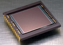 |
A CCD, shown here on the right (image
from
SBIG), shows a 1024x1024 CCD. The 1024
is the numbers of pixels per row and per
column. For a total pixel pount, use the
formula for the area of a rectangle - or row
x height = 1048576 pixels. This qualifies as
a "mega-pixel" CCD chip. |
A CCD is composed of smaller parts called pixels
- or picture elements. The resolution of a CCD chip
is the total number of pixels. They are organized in
rows and columns. When the CCD receives light, an
electric charge is collected by each pixel and
stores them until the image is downloaded.
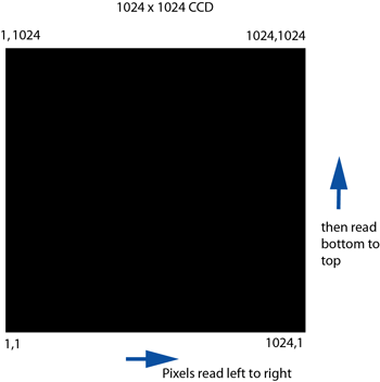
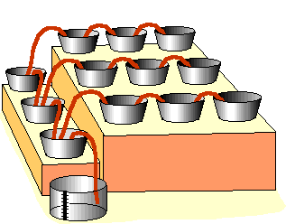
As seen in the image above, the charge of the
pixels is read a row at a times. The image below
shows an analogy of how the data from a CCD is read.
There are many definitions used to
define the capabilities of a CCD. The most important
of these is called Quantum Efficiency - or the chips
ability to see light. One of the factors that make
CCD's superior to film is its linear capability -
that is twice the exposure means twice the light,
unlike the reciprocity failure of film. Quantum
efficiency is defined by a percent out of 100 and
can be produced in graphical form:
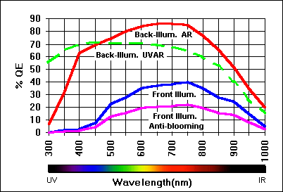
Image Credit
This graph also demonstrates
back-side illumination to front-side illumination.
These are terms that define the orientation of the
CCD chip. A CCD is coated with silicone and is
usually thicker in the front than the underside
(back side). This serves two purposes: protection
and stability. It was discovered that flipping the
chip over allows for more direct light on the pixel
elements, and shaving additional silicone from the
back allows for for light to reach the pixels, but
this process is exact and results in many failed
chips - hence the cost being in some cases twice
that of the usual chip. But the graph says it all,
they are more sensitive. Another type of CCD is
called "anti-blooming." If a pixel stores too many
electrons, they can spill over resulting in a
grossly over-exposed image.

The above example shows what
blooming does. An "anti-bloom" CCD contains
electronics that limit this behavior, but limits the
light grasp of the chip.
Other terms describing a CCD:
-
ABG - Anti-Blooming Gate -
reduces the blooming effects
-
ADC - Analogue to Digital
Converter - converts the electronic signal to
binary information
-
ADU - Analogue to Digital Unit -
a single count from a CCD
-
Bias - the background level of
the CCD
-
Bias Frame - a single image used
to counter the Bias from the image
-
CTE - Charge Transfer Efficiency
- the electronics ability to transfer the
electronic signal
-
Dark Current - thermal noise due
to heat build up on the chip
-
Dark Frame - an image used to
counter the effects of the Dark Current
-
Flat Field - an image used to
define the flaws of the CCD
-
Full-Frame Device - the entire
area of the CCD is exposed to light
-
Frame Transfer Device - only
half of the CCD is exposed to light
-
Gain - number of electrons per
ADU
-
Lumigen - fluorescent coating
used to improve UV response
-
Overscan - read out more pixels
than images, used for calibration
-
QE - Quantum Efficiency
-
Saturation - another name for
blooming
-
Shift Register - mechanism of
moving a charge around the CCD
-
Readout Noise - accuracy of the
pixel can measure the charge
-
Readout Register - location
where the charge is measured
-
Trapping Site - defect on the
CCD preventing electron flow
-
Well Depth - how many electrons
a pixel can hold prior to saturation, or
blooming
A couple of terms probably caught
your attention: Dark Frame, Flat Field, and Bias
Frame. These are images taken in addition to the
normal image. The purpose of these is for additional
calibration and reduction. Since the image from a
CCD is digital - hence binary - any defect in the
image can be cancelled out by using reduction
techniques. By subtracting the Dark, Bias, and Flat
frames from an image, a better image (and more
accurate image) results.
For more information of image
calibration, see my
Advanced Topics.
Back to Top |
